Newsletter 2020 Q4 Details
Advanced Encryption Standard
Advanced Encryption Standard (AES) is a popular and widely adopted symmetric encryption algorithm. It is used to encrypt and decrypt sensitive data and can be applied to both hardware and software. It is at least six times faster and uses a bigger key size (number of bits in the key) than earlier standards such as DES, triple DES, etc. This safeguards it against exhaustive key search attacks that are now more frequent due to increasing computing power.
AES has the ability to deal with three different key sizes (128, 192, and 256 bits), with each cipher (encrypted data) having a 128-bit block size. The number of rounds in AES is variable and depends on the length of the key. AES uses 10 rounds for 128-bit keys, 12 rounds for 192-bit keys, and 14 rounds for 256-bit keys. Each of these rounds uses a different 128-bit round key, which is calculated from the original AES key.

More Information: https://en.wikipedia.org/wiki/Advanced_Encryption_Standard
AES in Agnisys Flow
Agnisys supports AES as a separate IP in SLIP-G. This IP can be configured for AES encryption, decryption, or both and accordingly the encryption and/or decryption modules will be instantiated inside the top IP module. In addition, different data widths can also be defined.
During the encryption cycle, the encryption module will get the unencrypted (plain text) data from the bus write transaction. After encryption, the encrypted data will get stored on the registers. Thus on the read transactions, the user will get the encrypted data. Similar to the encryption cycle, the decryption module will get the encrypted data from the bus transaction during the decryption cycle. After decryption, the decrypted data gets stored in the registers. Thus on read transactions, the user will get the decrypted data. The key can be provided as a parameter or a register value to the encryption and decryption modules.
The current AES IP block supports 128-bit key size and data width up to 128 bits. Each encryption/decryption cycle takes at least 10 clock cycles to complete. During this period no new transactions are allowed into the AES block.

In the above diagram, reg_0, reg_1 … reg_n are the memory mapped registers whereas reg_buff_0, reg_buff_1, … reg_buff_n are the buffer registers of the memory mapped registers. The value of n depends upon the bus width. Currently the bus width and the register width must be the same.
The output from the AES block is always 128 bits wide. So, depending upon the bus width a certain number of registers will be used to hold the encrypted or decrypted data.
For example: If a bus width is 32 bits wide then four 32-bit registers reg_0, reg_1, reg_2, and reg_3 will hold the encrypted/decrypted data.
The write sequence for a 32-bit wide bus carrying 128-bit data will be:
1) Write 32-bit chunks of data to reg_buff_0, reg_buff_1, reg_buff_2, and reg_buff_3 buffer registers in 4 write transactions.
2) When a write transaction happens to reg_buff_3, a trigger or enable signal will be generated which then starts the required AES encryption or decryption module.
3) After the required encryption/decryption cycle, the processed data will be written to reg_0, reg_1, reg_2, and reg_3 registers.
The above approach also provides the flexibility for encrypting/decrypting data less than 128 bits.
For example: To encrypt 32 bits of data according to the AES algorithm, the user needs to write data to any of reg_buff_0, reg_buff_1, reg_buff_2 or reg_buff_3 and then trigger the AES module. The rest of the buffers will be filled with 0’s. By using this approach, users will also be able to change the position of the 32 bits within the AES generated 128 bits of data.
There will be no effect on the read transactions, which will work as for normal registers. The encrypted or decrypted data can be thus read in 4 read transactions on reg_0 … reg_3 for a 32-bit bus.
Conclusion
In present day cryptography, AES is widely adopted and supported in both hardware and software. As AES provides flexibility in terms of key sizes, it allows a degree of ‘future-proofing’ against advances in exhaustive key searches. However, this AES security depends upon its correct implementation and a good key management system. Currently, Agnisys AES IP only supports 128 bit key size, but it will be extended to 196 bit and 256 bit key sizes in the near future.
Hierarchical parameter overriding
Parameterization is one of the ways by which users can customize a component by specifying a generalized value of a component definition. According to the SystemRDL standard, “Parameter: A generalized value of a component definition that can be modified for each instance of the component.”
SystemRDL does not state anything about what output to generate for these parameters. It parameterizes almost all attributes of a component. But out of these, there are only a few values that can be reflected in various outputs such as Verilog and UVM.
Therefore, In IDS we have customizations at two levels:
- Specification level parameters (Generation Time Parameters)
- Output parameters (Elaboration Time Parameters)
Specification level parameters (Generation Time Parameters): These parameters are defined as described in standard SystemRDL 2.0 documentation. Their values are resolved by the preprocessor and/or compiler and appear as static values in the generated outputs, if applicable.
Output parameters (Elaboration Time Parameters): These parameters are mentioned in the specification but are not resolved by pre-processor or compiler. Instead, they are carried forward to the generated outputs (Verilog, UVM, C header, documentation) as parameters (not as resolved static values). They can be differentiated from the documentation level parameters by a ‘$’ sign in the beginning of their names. This is an Agnisys way of specification and is not part of the standard yet.
In SystemRDL the user can define N number of parameters at addmap, regfile, and register level and these parameters can be overridden from any top level to any lower level hierarchy. For example, a user can have a parameter at register level (example: param=0) and another parameter at reg_file (example: sec_param=1) so in SystemRDL the user can override the param value with the sec_param value.

In Verilog output, IDS creates modules for block/chip level hierarchies so register and reg_file level parameters in the RDL input are converted to localparam inside the block level module.
Verilog Output:

Naming convention of these localparam would be hierarchical up to the block level to make them unique inside the block module.
For example, localparam name of param used at register_1 would become Ref_sec_Reg1_param, following the below naming convention:
<hierarchical register instance name>_<parameter name>, here Reg1 is register instance name
Obviously, it only makes sense to change a few values at elaboration time: reset value, component offsets, field bits size, repeat value, and hdlpath. Items such as names of registers, access types, etc. are not needed to be changed at elaboration time.
Conclusion
By using the above methodology, we can differentiate between the top level parameters at the addrmap with parameters at register and reg_file and override them from the top. Also, users can override the value of individual register and reg_file parameters at elaboration time. These parameters help you make a more versatile and reusable specification. With the IDS enhancements of output level parameterization you also get versatile and reusable output code in RTL, UVM, C header, and documentation.
SECDED in IDS
Functional safety is very vital in the designs today. There are various techniques that are used in the industry to provide this capability. The designs that are covered under it tend to automatically prevent failures and control them when they occur, depending upon the mechanism being used. It helps designers to ensure that the system can execute specific functions correctly, even under unfavorable conditions.
The technique that we will discuss here is “SECDED”.
SECDED stands for Single Error Correction, Double Error Detection. Sometimes, data in a register may get corrupted due to cosmic rays or some other factor. There are many error detection methods that can be used to detect the error and then rewrite that data. But sometimes the error is only 1-bit and it is cumbersome to do the write process again. So, in such cases SECDED is used.
It is basically a Hamming code, which encodes the data by adding parity bits to it. This encoded data is then transmitted. At the receiver’s end, parity is again calculated using the same method that is used at the transmitter’s side. These parity values are XORed with the transmitted parity to evaluate if the data is corrupted or not. Corrupted data is marked by an error signal. If an error signal indicates a single bit error in the data then the XORed result will point to the bit that is corrupted and the same can be corrected at the receiver’s end. For a 2-bit error, SECDED detects but cannot correct the error, so it alerts the user to take up some preventive actions.
In IDS, SECDED is handled for both internal as well as external registers.
For write operations on internal registers, the data is passed to the SECDED encoder. This module generates the SECDED encoded data. The data bits from the encoded data are stored in the register and the parity bits, depending upon the user information, are stored in the internal buffer. IDS also provide the flexibility to output the parity bits. By default, parity bits are stored in an internal buffer.

Fig1. Write operation for internal registers
Write operations for external registers work in the same way as that of internal registers. The only difference is that instead of storing data and parity bits internally, they are routed to the memory.
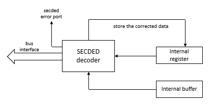
For read operations on internal registers, the data is first passed to the SECDED decoder stage. This module checks for the occurrence of any SECDED error. If a single bit error is detected then the decoder module corrects the corrupted data and passes it on to the bus interface. Also, at the same time, it updates the stored corrupted data.

Fig2. Read operation for internal registers
Whenever an error is detected by the decoder, it is reflected on the “secded_error” port.

n IDS, users also have a flexibility to route the double error detection to the bus interface.
Read operations for external registers work in the same way as that of internal registers. The only difference is that when a single bit error is detected then the decoder provides only the correct data and does not issue any transaction to the external memory for correcting the corrupted data.
Conclusion
SECDED proves to be a very useful technique where single bit error is detected, and it is inconvenient to rewrite the entire data again. SECDED in IDS is supported for both internal and external registers. However, single bit correction of the stored data only happens in case of internal (register based) storage.
TMR with error injection, detection and correction
Systems have been expanding widely in terms of both capabilities and resources. One of the major concerns, in the designs, is the occurrence of a fault in the system. A fault is a violation of some form in the normal (expected) working of the system. A fault can eventually lead to a single failure or multiple failures in the system. The fault can occur due to hazardous environmental conditions or due to cosmic rays that can knock out a storage bit in a system. In order to avoid this, there is a need to eliminate or control the fault.
The technique to provide tolerance against such single hardware component failure is triplication of the component, called Triple Modular Redundancy (TMR).
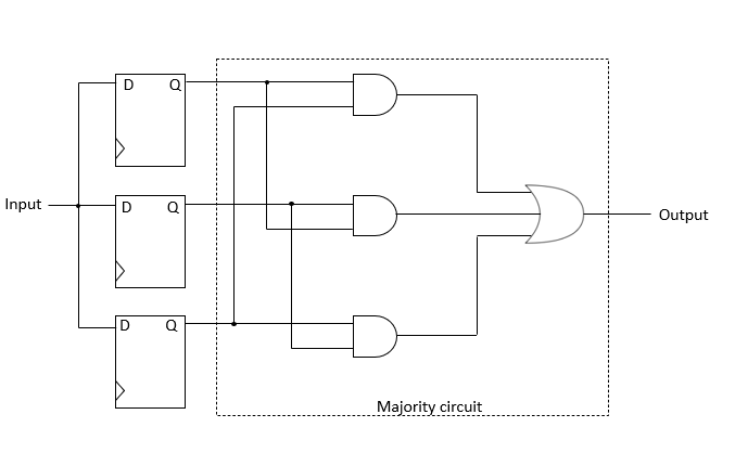
A TMR register is a mitigation technique, to protect digital logic from the Single Event Update (SEU) in space-borne application, communication, ECC memories, etc. It uses three identical logic circuits performing the same task in parallel with corresponding outputs being compared through a majority voter circuit. If any one of the three systems fails, the other two systems can correct and mask the fault.

Figure 1. TMR Logic Diagram
In IDS, the TMR functionality can be achieved with the help of the ‘tmr’ property, which when applied on any register triplicates the input logic as shown in Figure 1 above. The final output is based on the majority voter circuit where two correct values will “outvote” an incorrect value using the logic function below for software and hardware write operations.
Logic function: Output = I1I2 + I1I3 + I2I3
Clearly, the TMR register can completely mask the failure of only one hardware unit. TMR is particularly suitable for transient faults, because in the basic TMR the voter does not “remove” the faulty unit after an error occurs. Due to this, the reliability of the TMR system becomes lower once a failure occurs.
Therefore, some enhancements have been made in TMR for error injection as well as detection and correction, which are much needed in this model for having a more reliable system.
The TMR register described so far silently corrects the errors. With the IDS property ‘tmr_error’ the user can also detect an error, and an active low signal is generated to indicate the presence of an error. This error is corrected in the next cycle where the bit flipped is auto corrected.
TMR error logic: Output = ( ~ ( | (I1 ^ I2) | (I1 ^ I3) | (I2 ^ I3) ));
Another IDS property ‘tmr_error_inject’ can perform error injection so as to check for faults during functional mode of the chip. The error can be injected based on an additional input signal, where one of three systems is injected with an error. This error can be detected and corrected in the next clock cycle with the tmr_error logic.
Conclusion
In TMR, three identical logic circuits (logic gates) are used to compute the same set of outputs. If there are no circuit failures, the outputs of the three circuits are identical. But in the case of circuit failures, the outputs of the three circuits may be different. In order to make TMR registers reliable they have been enhanced with error injection, detection and correction logic with the help of various IDS properties.


