Agnisys now Supports Complete Validation of Special Registers
Special registers are complex in nature and are designed based on their applications. All the registers are validated for both hardware and software access. Agnisys uses the Xilinx® platform for analysis, synthesis, and simulation of special registers. For validation of special registers, we use the Xilinx ZedBoard®.
The tool used for complete verification and validation process of special registers is Xilinx VIVADO® 2014.2 along with a software development kit.
Using Xilinx Zedboard and Xilinx VIVADO 2014.2 we were able to successfully validate the following registers.
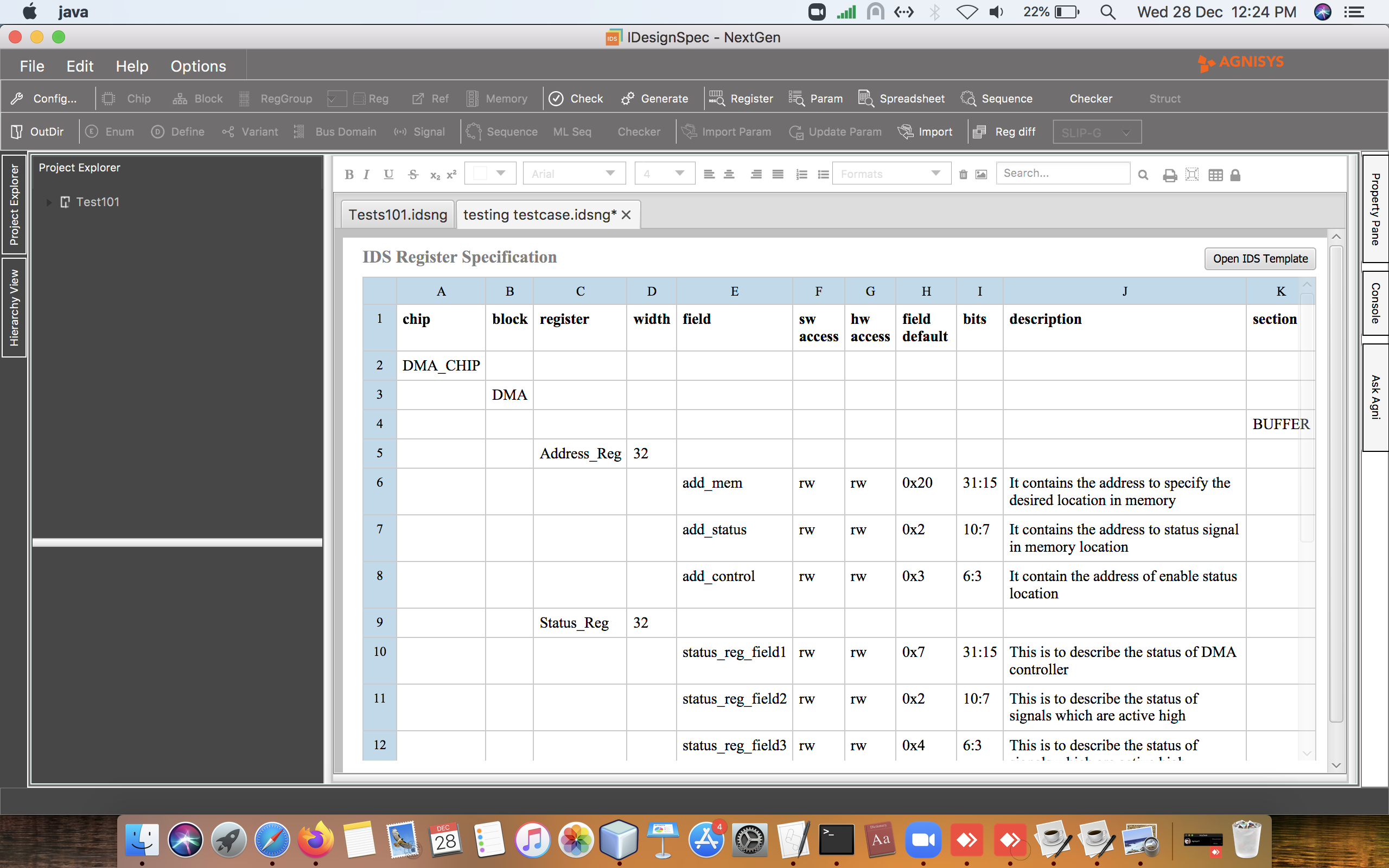
- Counters
- Lock register
- Register array
- Shadow register
- Triple modular redundant register
- Trigger buffer register
- Alias register
Sequential process involved in the validation
- Register Transfer Level, generated by our tool IDesignSpec (IDS), is converted into IP Package. Before packaging RTL as an IP, it is verified that the design is synthesizable and simulates as per the protocol
- IP Package is then interfaced with ZYNQ processing system
- Bit file is generated which basically contains the necessary information to properly configure the device
- This bit file is then dumped onto the ZedBoard
- To program the ZYNQ processing system, we use Xilinx tool software development kit
- Sequences are written using our tool ISequenceSpec (ISS) in the Xilinx tool software development kit
- These set of sequences can either run individually or simultaneously
- The corresponding output generated after running sequences can be either verified by LEDs on ZedBoard or by checking software development kit variables
- Alternatively, the output can also be verified directly by checking values of registers in XMD shell
IDesignSpec generated register transfer logic acts as an input for Xilinx VIVADO 2014.2. Similarly, ISequenceSpec generated sequences act as an input for the software development kit.
ISequenceSpec also generates a header file. This file contains information such as offsets, masks and addresses of the registers, which is included in the main file. Sometimes, both the files are combined in a single file during validation, but the tool ultimately generates a separate file for both. Generated sequences are fired by an ARM® processor which is builtin the ZYNQ processing system.
Given below is a pictorial representation of the validation process which takes place in counters.
Hardware event: VIVADO Design

Software Embedded C code in Xilinx software development kit

UP/DOWN Counter: VIVADO Design

Software Embedded C code in Xilinx software development kit

Software events: VIVADO Design

Software Embedded C code in Xilinx software development kit

A similar process is implemented for the validation of other special registers.
Functional Safety using IDesignSpec for the modern Auto-Industry
Functional Safety is the new buzzword within Electronic Design. From staying up-to-date on the latest standards to managing all the associated data, complying with functional safety requirements has traditionally been a time-consuming, manual effort.
Transforming this process by incorporating cyclic redundancy check and parity checks for system-on-chip (SoC) and system designs adhering to ISO 26262 standard has given a new edge to functional security in electronic design. One of the most important elements of functional safety as it relates to the embedded systems that are now present in modern day vehicles relates to fault detection. Simply put, regardless of where the fault comes from, the system’s ability to both A) identify it, and B) resolve it in the minimum time span possible is and will always be the goal. Agnisys aims to provide an end-to-end functional safety solution reducing the automotive compliance effort.
Enter: IDesignSpec™
Because of the current state of the industry, along with trends that paint a better picture of where the industry itself is headed over the next decade, IDesignSpec™ has been enhanced in a wide array of ways to cater to these and other growing needs. A host of unique, new features have been added to better integrate aspects of functional safety not only throughout all phases of the system development but in a way that still maintains compliance with the ISO 26262 standard.
Here Figure (1) demonstrates how IDesignSpec provides an end-to-end functional safety solution reducing the overall automotive compliance effort.
Detailed Process – Glimpse of our live demonstration at DAC 2018
The hardware consists of a Xilinx® ZedBoard™ in which we have a sniffer logic for error detection and cosmic logic for inducing an error
1. Under a normal scenario when sniffer logic is OFF, the car follows a normal path as shown in Figure (1). When a cosmic error is induced the car deviates from its original path to an error path, which may lead to an accident as illustrated in Figure (1).
2. As soon as we turn ON the sniffer logic and induce a cosmic error, the car automatically detects the error and uses sniffer logic and follows a safe path.
Figure (1)

How Cyclic Redundancy Check (CRC) Works
CRC acts on a piece of data which is calculated at the time of transmission (write transaction) and checked at the receiver time (read transaction). A CRC Generator divides the data by a polynomial given by the user and the remainder of the division is called the CRC checksum, which is appended to the data.
The CRC Checker divides the data (data along with CRC checksum) by the same polynomial. If the result is 0, then the received data has no error and if the result is a non-0, then an error has occurred in the data.
CRC in IDesignSpec
CRC/Parity is used to guarantee functional safety. IDesignSpec supports CRC and Parity to automate the process and reduce the compliance effort adhering to ISO 26262 standards.
Ways to create CRC in IDS
1) {crc= polynomial}
Polynomial – Represents the CRC polynomial in form of bits. The whole register will be treated as a data (message bits). CRC checksum will be stored internally in the RTL
2) {crc = polynomial, CRC sum field, crc data field}
Polynomial – Represents the CRC polynomial in form of bits
CRC sum field – Represents the CRC field bits after the calculation
CRC data field – Represents the message field bits
3) {crc_error = Signal}
This property implies that a checker has been created. If crc_error property is not specified, then the checker has not been created.
4) {crc_seed = seed value} This property represents the initial value of checksum
Examples of CRC in IDesignSpec
(1)

1. Here the polynomial is x6+x4+x3+x
2. Data is 25:0 bits
3. CRC is stored in bits 31:26
4. The error bit will be field “F” of “Reg1”
5. The default value of CRC Generator checksum is 110111
(2)

1. The polynomial is same as the previous example
2. Data is 31:0 bits
3. CRC is stored in bits 37:32
4. Note that the CRC bits are not shown in the register template
5. The error bit will be field “F” of “Reg1”
6. The default value of CRC Generator checksum is 110111
Parity
A parity bit, or check bit, is a bit added to a string of binary code to ensure that the total number of 1-bits in the string are either even or odd.
Following are the properties of parity
1. {parity=type, parity field bit, message field bits}
Type represents the parity type. It can be of two types odd/even
Parity field bit represents the bit of the parity
Message field bits represents the whole data on which the parity is calculated
2. {parity=type}
Type can be odd or even
Parity bit will be stored internally in the RTL
Message /data represents the whole register bits
3. {parity=type, register bit}
Type represents the parity type. It can be of two types odd/even
Register bit represents the bit of the register which will store the parity
Message /data represents the whole register bits
4. {parity_error= Signal}
Parity error (generated in case of read) will be stored in the signal
If parity_error property is not specified, then the checker is not created in RTL
Examples of Parity in IDesignSpec
(1)

1. This example will calculate the odd parity
2. Data is 30:0 bits
3. Parity bit is stored in bits 31
4. The error bit will be field F of Reg1
(2)

1. In this example, Parity of the eeprom register is stored in the F1 of the Reg1
2. The error signal of the parity goes out on Signal1
Sniffing engine
1. Sniffer engine enables the parity checker, check the result. Sniffer optionally sets an error flag and address of failed register.
2. The property of sniffing engine is {ecc_sniffer=counter_time}
The value of this property specifies the time after which sniffer will recalculate the ECC of entire address map.
1. Eg – {ecc_sniffer=20}
In this example, the time difference between the sniffing cycle will be 20 clock cycles
2. In case of SW read and sniffer read, the priority is given to SW read
3. The error flag of the sniffing engine will be same as parity error flag
4. The address to represent the location of the error will be a HW port.
Block diagram for sniffer

Why IDesignSpec
Advancements like IDesignSpec, help offer an essential solution by not only reducing the overall automotive compliance effort by giving teams the ability to work “smarter not harder”, but also provide a new (and pivotal) edge to functional security.
Agnisys now supports Duolog format for IDesignSpec – Create executable design code from the specification
The input format of Duolog is now supported by IDesignSpec with outputs including Verilog, UVM, CHeader, and SystemC. The outputs generated are compatible with both Duolog as well as IDesignSpec formats. We have incorporated multiple special enhancements and new features to support Duolog compatibility and making the output generation 10x faster.
Users can create and validate code from the specification itself and experience its benefits with faster RTL and more versatile UVM. We have created a drop-in replacement for several outputs like Verilog, Verilog header, SVheader, Cheader, UVM, etc. for a few of our Duolog users.
Out-of-the-box Features
1. Implementation of advanced properties for our users. For instance; adding an additional map, same as default map in UVM for multiple bus domains, making UVM relocatable from one chip to another chip.
2. Implementation of System level C-test as one of the outputs for faster and effective results
3. Duolog compatible system level C-test enables users to generate both UVM sequences and C-test simultaneously with the same specification in a fraction of seconds. Hence, tests as well as sequences, are well evaluated and validated
4. Another interesting feature which we have incorporated is “parity” for bus data and register data.
Benefits for our Users
1. We now support Duolog’s “input excel document” and output format (-in_third_party d for taking Duolog input, and -out_third_party d for generating Duolog Verilog and UVM outputs).
2. We have successfully matched the Duolog output, right from flattening of registers and regGroups to creating an external widget that will add a delay to the IP_READY signal for external registers in Verilog and generate extra code (set_compare, option.per_instance, set_check_on_read etc.) to make UVM relocatable in UVM output.
3. For Verilog, we have a command line option that makes the bus port case sensitive (bus_port to UPPER/LOWER using “-bus_port_case upper/lower”). In addition, we have a command line to specify the default reset using “-default_reset async/sync”. We have the capability to limit the generation of read and write error that is generated in IDesignSpec by default using “-rtl_no_error”. We have created non-piped axi_widgets (AXI4Lite and AXI4Full with burst) which are not supported in Duolog format.
4. For UVM, we have added code for UVM_CHECK (option.per_instance, set_check_on_read, set hdl_paths in uvm.configure to null, etc). We have changed the block class similar to Dulog format (“abc_block” to “abc_t”). We have created an additional property to generate multiple regmaps. We now support “vertical_reuse” property, that will make the UVM relocatable.
5. In General, we have created a Duolog compatible SystemC output. User can create multiple PDF and svheader file for each block using command line option “-if_pdf” and “-if_svheader” respectively. We also support “-top_property” to specify any property at the top level module and “-mbdc” to mention the multiple, bus domain table on the command line for inputs that don’t support multiple bus domains in the register format, for example IP-XACT.
“IDesignSpec always surprises us with its functionality and vastness in usability.” – IDesignSpec user
SystemVerilog Decoder Ring using Machine Learning
An assertion, in the context of a programming language, is a statement that validates assumptions or checks condition in a program. An assertion, for example, helps notify the user if some legal or illegal combination of values of internal program variables have occurred.
SystemVerilog has integrated a set of constructs that help a user build assertions and closely couple them with the rest of a design or verification code. Assertions are primarily used to validate the behavior of a design, a check embedded in or bound to a design unit during simulation. Warnings or errors are generated by the failure of specific condition or sequence of events. Assertions are used to check the occurrence of a specific condition or sequence of events to provide functional coverage.
Writing assertions can be a tedious job for engineers. It is difficult to interpret an assertion written in a specification or in a code. Engineers often find it difficult and time-consuming to understand an assertion already written in a specification or even to write an assertion. Sometimes, after the assertion is written, the user feels the need to validate the code to avoid last-minute issues.
It’s every engineer’s dream to have a decoder which will make their life easier.
The SystemVerilog Assertion Decoder Ring
Keeping in mind the above-mentioned problems and challenges faced by engineers while writing, testing, or interpreting assertions, we have created a new solution, the SystemVerilog Assertion Decoder Ring (SDR). We call it this because it can feed an assertion and provide the user with its output in English, or it can take the English language as an input and provide a corresponding output assertion for it.

How does it Work?
The SDR solution leverages a Machine Learning mechanism. The SDR engine has been fed with numerous different types of assertions. The level of assertion varies from simple to difficult. The focus of SDR is to decode the concurrent assertion.
Different assertions written in the format described by the SystemVerilog standard is first parsed and converted into a machine learning engine trainable form. A machine learning algorithm then runs on this parsed data to train the engine for its corresponding output in English. The machine learning algorithm is also trained on data in the English language which contains the description of different concurrent assertions with its corresponding output assertions in SystemVerilog.
Both these functions are clubbed together to create the SystemVerilog Assertions Decoder (logic) Ring that can take input as SystemVerilog assertions and provides the output as its explanation in English and vice-versa.
A simple example of SDR is shown below
SDR Input:
$rose(a) |-> (a throughout b [->1]) ##1 !a
SDR Output:
Whenever a goes high, a must be high until b is asserted and after 1 clock cycle, a must be low
SDR can be used for various purposes such as to interpret assertions, write different assertions, and validate the assertion written for its correctness by checking its description in English. Hence, this property holds the potential of making the complex life of an electronics engineer much simpler.