Thoughts and Insights on SystemRDL Loopholes
The Accellera SystemRDL supports the full project cycle of registers from the specification, model generation, and design verification to maintenance and documentation, and minimizes the problems encountered in describing and managing registers. Typically, the system architect or hardware designer creates a functional specification of the registers in a design. This specification is then used by other members of the team including software, hardware, and design verification. Each group uses the specification to create representations of data in the languages they use in their aspect of the chip development process. This includes RTL, UVM, C/C++, HTML or PDF.
During the verification and validation processes, bugs are often encountered which would require the original register specification to change. When these changes occur, all the downstream data have to be updated accordingly. This process is typically repeated numerous times during chip development. In addition to the normal debug cycle, there are two additional aspects that can cause changes to the register specification. First, marketing requirements can change, which require changes to the register specification. Second, physical aspects, such as area and timing constraints can also drive changes to the register specification.
These challenges often result in a low-quality product and waste of time due to incompatible register data and views. With the use of SystemRDL and a SystemRDL compiler, users can save time and eliminate errors by using a single source of the specification and automatically generate the required data for design and verification.
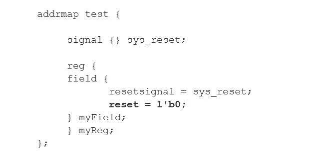
Consider the following simple SystemRDL model:
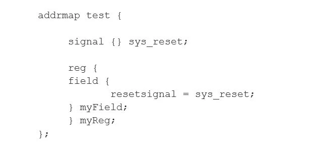
While being a perfectly valid and compilable register model as per requirements of the Accellera SystemRDL standard, this definition hides a potentially harmful issue. According to the standard, by default, the reset value of fields shall be unknown, basically, ‘x’ in Verilog/VHDL terms. So, if no reset value is given, the field is not being reset, even if it has a ‘resetsignal’ associated. In ASIC chips it is critical to have deterministic reset behavior for every register. The same requirement applies to many cases of safety-critical FPGA designs, where a predictable and controllable reset state is highly valuable.
So, a mistake to specify a reset value at the level of SystemRDL description would propagate unnoticed to the generated RTL implementations.
It will likely be spotted later down the design flow at the level of synthesis or RTL linting tools, however, the earlier the problem can be identified, the less time is wasted. Although, spotting this type of mistake visually in an industrial-scale register specification would not be easy even for experienced designers.
Agnisys new SystemRDL compiler can prevent this type of mistakes very early in the specification development flow by displaying rich compilation warnings:
WARNING: example.rdl(8): Property ‘resetsignal’ is effectively defined in the instance ‘test.myReg.myField’, but the implied ‘reset’ property is not effective. The field is not going to be reset properly.
A correction of the issue looks very simple:
Seeing that feedback before synthesis and simulation of the incorrect RTL implementation could save the designer many hours.
Although SystemRDL is a useful industry standard for capturing the register information. We have found few loopholes in SystemRDL2.0 standard documentation and would like to know your perspective about Structs in Constraints and Stride Operator (%=).
Structs in Constraints
Consider the example below

In the above example, the definition is completely valid for SystemRDL 2.0, but it violates some of the other chapters.
6.3.2.1.2.a) A struct can be used within user-defined property definitions, parameters, arrays, and other structs.
None of the examples involving structs in the standard uses those outside of UDPs or parameter declarations.
On the other hand, item 14.2.1 clearly restricts constraint expressions to reference fields only:
14.2.1 …A constraint expression is a value-based condition on one or more fields visible from the scope in which the constraint component is defined. The field references may only be to a field instance and not a property of the field. Fields can also be specified using the hierarchical operator (.) (see 5.1.4).
If the constraint is instantiated inside a field, the this keyword can be used to reference the enclosing field.
So, the example is confusing. Our guess is that the “pixel value” structure instance should be denoting a field of the struct type. Currently, the fields can only be of single-bit or vector type in the RTL implementation. Something like SystemVerilog packed struct could probably represent the intent of this example.
Then field references would map to something like slices, depending on the struct’s member offset within the struct:

Stride Operator ( %=)
The property stride operator elaborated in the System RDL documentation is also a little confusing. Consider the following example:
In case you have a register with repeat of 10, depicted as : Register[10]
So a register Reg1 occurs for the first iteration. If the value of the stride is 5, then after an empty space of 5 the next register will occur.
Next register Reg2, occurs for the second iteration. After that an empty space of 5 address spaces exist before the next register to exist
Similarly, Reg 3 at the third iteration, and an empty space of 5 and so on for ten iteration.
The documentation does not elaborate on how the empty space will be utilized. We have plenty of questions like:
- Can this space be used instead of leaving it empty, as empty space is never good for a design.
- Is overlapping allowed at the empty space?
The above-mentioned issues are just a glimpse of what we as engineers saw as loopholes in the documentation. There are still many more which we have explored, we will be covering the same in the next few blogs.
To read more about SystemRDL and its functionality and comparison with other languages, please refer to the links mentioned below:
https://www.agnisys.com/systemrdl-functionalities/
https://www.agnisys.com/newsletter-yaml-systemrdl-and-ralf-construct-comparison-for-registers/
https://www.agnisys.com/newsletter-ip-xact-vs-systemrdl-constructs-comparison-for-registers/
https://www.agnisys.com/systemrdl/
Let’s start a discussion regarding these two loopholes. Send us an email at info@agnisys.com or marcom@agnisys.com.
Security Design Strategies in IDesignSpec
Security is one of the most important aspect of SoCs/IPs in the Internet-of-Things (IoT) era. Securing your SoCs/IP is critical for providing authentication, confidentiality, integrity, non-reproduction and access control to the system.
Nowadays IPs have become the major building block of complex and highly-integrated SoCs, in which various IPs such as memory, Bluetooth, Wifi or HDMI are found in almost every modern electronic device. This has evolved into one-chip solution that manages many of the functions, features, and applications that are found in the ubiquitous sea of today’s electronic products.
For securing sensitive and critical data in the chip, various security design strategies are used as building blocks to develop more advanced security features. Chip designs should be secured, protected and should not be affected by any misconfiguration at the designer’s end.
Protection Support
In protection support mode, areas of memory could be physically isolated by the processor itself to prevent illegal writes to other programs running in memory at the same time. Before the introduction of protection mode, any program could be accessed by any area of memory, as multiple programs could be running in memory at the same time. In such cases, the entire system may get down. Some buses provide access permission signals that can be used to protect against illegal transactions. Access permissions for reading accesses/write accesses on registers are:
- privileged/non-privileged
- secure/non-secure
- data access/instruction access
We can also protect the register against modification of its value from the hardware (register port) side.
Secure Configuration
We can protect the register configuration by a software write access of a register, another register field, an expression consisting of different register fields or some external signals.
IDesignSpec™ provides security at IP level by using a special register where misconfiguration of a register can be tamed. The software read and write access of a register or register’s field can be locked based on the value of another register field or an expression consisting of different register fields or some external signal (declared as input in signals’ table). Such register for which the write access is locked is called as “Lock Register”.
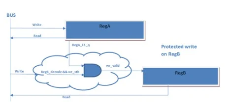
igure 1. Lock Register
In Figure 1, the register “RegB” is locked if the value of the field “F1” in register “RegA” is equal to any non-zero value, otherwise “RegB” is unlocked.
We have another scenario in Lock Register in which the software write access of register “RegB” is locked if every condition within the lock expression evaluates to true.
Protection Signals in IDS
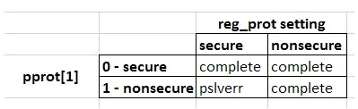
Figure 2. Protection signals
The protection signals are also handled by IDesignSpec. You can protect the register from the software side (or anything that’s coming from the bus). The read and write access from the software side is controlled by protection signals of their respective buses. We have possibilities such as:
- priv, secure
- unpriv, nonsecure
- priv/unpriv
- secure/nonsecure
When a secure transition comes from the bus then the transition will be completed in a secure/nonsecure register. When a nonsecure transition comes from the bus then it generates a slave error signal in a secure register and the transition will complete in a nonsecure register.
Future Scope
Power analysis attacks are a major concern in the protection of secret data stored in cryptographic devices. It is a class of side-channel attacks based on power consumption measurements. For increasing the security of cryptographic devices against PAAs, apart of IDesignSpec’s roadmap is to implement a secure double rate registers (SDRRs) as RTL countermeasure.
To expand the security of cryptographic devices against power reduction analysis, secure dual rate register with AES is introduced. It stores the original data and random data at the same time so that less time is required.
For design strategies for applications that requires functional safety, please refer to the link mentioned below, which talks about CRC and Parity features using IDesignSpec – https://www.agnisys.com/functional-safety-using-ids/
RISC-V TileLink Bus Protocol Support in IDesignSpec™
New generation SoCs in deep learning applications require new types of processor architecture, and the open-source RISC-V ISA is picking up a lot of steam. As we know, Moore’s Law has ended and standard CPUs are not able to meet the performance and power requirements of new generation SoCs. Domain-specific architectures with the help of open-source concept will play a critical role to push innovations forward. TileLink is an open-source bus-protocol with low latency and cache-coherent shared memory designed for RISC-V, and it’s now supported in IDesignSpec™ .
To establish communication between multiple processors and peripheral slaves (IP, memory or external registers), the system needs a set of protocols, which are followed by all three types of buses (address bus, control bus, data bus), known as bus protocol.
The industry has many standard buses such as, serial bus (SPI, I2C) and the parallel bus (AMBA-APB/AHB/AXI, WISHBONE). Serial buses are used for serial communication and have one pin for all three buses (address, control and data). Parallel buses are used for parallel communication and have multiple separate pins for all three buses.
Every parallel or serial bus has their specification based on its application, for example, APB is used for low peripheral application where as AHB is used for high-frequency transaction and AXI is used for cache. So every bus protocol has some advantages and limitations.
As per requirement, bus protocol functionality changes as technology advances with time. Hence, for the better response and industry requirements, RISC-V microprocessor is invented, which is completely open-source. RISC-V supported a new bus protocol, TileLink, which not only has all the previous functionalities but also has some more new features.
TileLink is an open source bus and provides tightly coupled and low latency for Soc buses. It is used to connect the processors, co-processors, accelerators, etc. TileLink provides fast and scalable interconnection which further provides high throughput transfer. TileLink was designed specifically for RISC-V but also supports other ISAs.
It has three levels:
- TileLink Uncached Lightweight (TL-UL): Only supports read and write operation.
- TileLink Uncached Heavyweight (TL-UH): It adds a multi-beat message, atomic and hints operation to TL-UL.
- TileLink Cached (TL-C): It adds cache block transfer and channel B, C, and E to TL-UH.
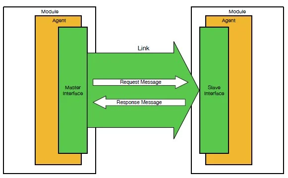
TileLink transfer messages from one agent (an active participant in the protocol that sends and receives messages in order to complete operations) to others by link which contains channels (a one-way communication connection). Every channel has some set of signals to process the message.
The channel has signals as:
- Control signals (C): opcode, param, size, source, address, sink.
- Data signal (D): data, mask.
- Final signal (F): error.
- Valid signal (V): valid.
- Ready signal (R): ready.
Working on the TileLink bus protocol
Whenever communication takes place between the master and slave – master initiates the transaction and the slave responds to the master. In the case of TileLink – Channel ‘A’ requests slave’s channel for the transaction and Channel ‘D’ is the response channel to the corresponding request message.
Transactions
PutFullData and Get:
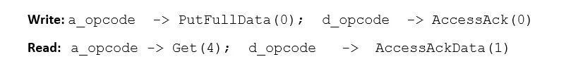
PutFullData operation ‘a_valid’ signal is asserted with ‘PutFullData’ message from the master, through a channel ‘A’, with all control signals as shown in the diagram. At the same cycle, the slave receives it by asserting ‘a_ready’. On the next cycle, the response channel asserts ‘d_valid’ from the slave side with the message ‘AccessAck’, then master accepts the response by asserting ‘d_ready’ signal.
In Get operation ‘a_valid’ signal is asserted with ‘Get’ message from the master through a channel ‘A’, with all control signal as shown in the diagram. At the same cycle, the slave receives it by asserting ‘a_ready’. On the next cycle, the response channel asserts ‘d_valid’ from the slave with the message ‘AccessAckData’, then master accepts the response by asserting ‘d_ready’ signal.
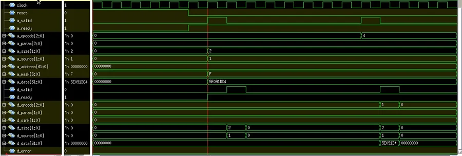
Figure2. Generated Waveform – In Case Of PutFullData and Get
- PutPartialData and Get:
In PutPartialData operation ‘a_valid’ signal is asserted with ‘PutPartialData’ message from the master side through a channel ‘A’, with all of the control signals as shown in the diagram. At the same cycle, the slave receives it by asserting ‘a_ready’. On the next cycle, the response channel, asserts ‘d_valid’ from the slave side with the message ‘AccessAck’, then master accepts the response by asserting ‘d_ready’ signal.
In Get operation ‘a_valid’ signal is asserted with ‘Get’ message from the master side through a channel ‘A’, with all of the control signals as shown in the diagram. At the same cycle, the slave receives it by asserting ‘a_ready’. On the next cycle, the response channel, asserts ‘d_valid’ from the slave side with the message ‘AccessAckData’, then master accepts the response by asserting ‘d_ready’ signal.
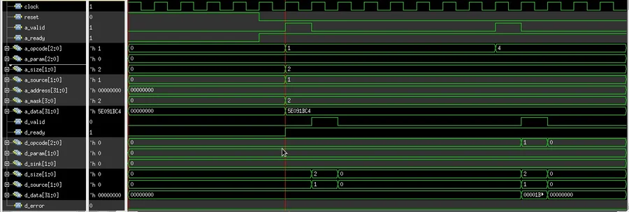
Figure 3. Generated Waveform – In Case of Partial Read and Write
The difference between the ‘PutFullData’ and ‘PutPartialData’ message is the value of ‘a_mask’ i.e. with ‘PutFullData’ write all byte on data bus but ‘PutPartialData’ does not write all bytes on the data bus.
Error Transaction
Sometimes, we access location that does not exist or locations with limited access like a read-only or a write-only register. Now, if we perform any message on this location then the error will generate instead of the requisite data.
Here with an error transaction, the response channel generates the error signal ‘d_error’.
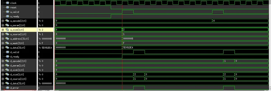
Figure 4. Generated Waveform – Error Transaction
Delayed Transaction
Sometimes, we access an external location that responds after some time i.e. delayed response. Now if we perform many messages on such location then the response channel will be delayed for some cycle with respect to the external location.
Here, with a delayed transaction, the response channel will be delayed for one cycle with respect to the external location. So, the slave asserts the signal ‘d_valid’ delayed by one cycle.
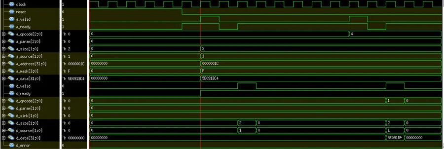
Figure 5. Generated Waveform – Delayed Transaction
Hierarchical Decode
Address decoding makes the memory or register function at a unique section/partition of the memory/register map. Without an address decoder, only one IP block can be connected to a processor, which would not be useful for today’s SoCs.
For each IP Block, addresses can be decoded in two ways:
- Absolute decode – where all address bits are decoded for each block. This functionality is currently set by default in IDesignSpec.
- Hierarchical decode – where the address bits are divided into two parts, the MSB part which is used to decode the block and the LSB part which is used to decode the register being addressed, once the block address (the MSB part) is selected.
Hierarchical decode is advantageous because of the following reasons:
- The entire address bus does not need to be routed to all the blocks in a chip, this reduces the routing congestion.
- Since decode is happening only at one place and select lines are used to signal the selected blocks, the power consumption is low.
- A select line is used for each block that indicates that the block’s registers are selected, this has the advantage that the address offset does not need to be passed as a parameter to the block. This, in turn, has the advantage that the same physical block can be reused multiple times.
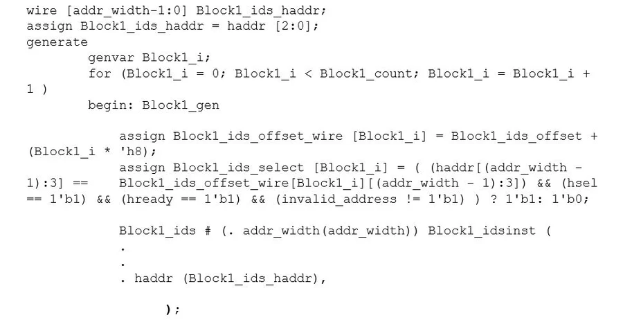
For this, IDesignSpec has a property “hierarchial_decode=true”. This property is applied at the chip, as illustrated below:
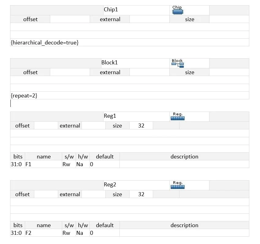
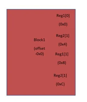
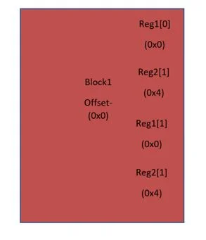
As an example, if there is a repeat of 2 on the block then registers of iteration ‘0’ are at 0x0 and 0x4 and registers of iteration ‘1’ are at 0x08 and 0xC. By default, register map at the block level in IDesignSpec is as shown below:
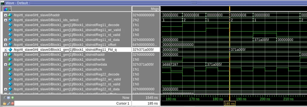
The generated waveform is shown below.
With Hierarchical Decode
The block structure will be re-used and also the register’s address structure will remain the same. Considering the same example if there is a repeat of 2 on the block then registers of iteration ‘0 ‘ and ‘1’ are both at 0x0 and 0x4. Register mapping of the blocks with hierarchical decode is as shown below.
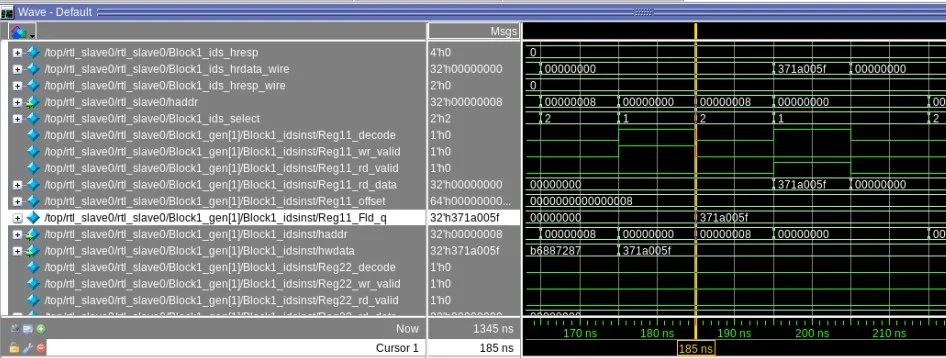
The generated code from IDesignSpec is shown below.