Newsletter 2021 Q4 Detailed Content
UART in SLIP-G™
SLIP-G™ (Standard Library of IP Generators) from Agnisys offers configurable standard IP generators as an extension to its addressable register generator tool. These IPs are designed to be easily customizable and configurable to meet any SoC requirement. IDS automatically creates register specifications and generates RTL for standard IPs. All SLIP-G™ generated IPs are characterized by generation time parameters. Users can choose these parameters based on their specific needs.
A new IP, UART, is added in the standard library.
Universal Asynchronous Receiver Transmitter (UART)
UART stands for Universal Asynchronous Receiver/Transmitter. This block provides the controller with the functionality of asynchronous serial data transfer.
The UART that is going to transmit data receives the data from a data bus. The data bus is used to send data to the UART by another device like a CPU, memory, or microcontroller. Data is transferred from the data bus to the transmitting UART in parallel form. After the transmitting UART gets the parallel data from the data bus, it adds a start bit, a parity bit, and a stop bit, creating the data packet. Next, the data packet is output serially, bit by bit at the Tx pin. The receiving UART reads the data packet bit by bit at its Rx pin. The receiving UART then converts the data back into parallel form and removes the start bit, parity bit, and stop bits. Finally, the receiving UART transfers the data packet in parallel to the data bus on the receiving end.

Features Offered
Following features are offered by UART block:
- 5, 6, 7, or 8 bits per character (means data bits in a single packet)
- Configurable parity bit (odd or even or none)
- Configurable baud rate
- Full duplex
- 1 or 2 stop bit detection and generation
Data Frame
UARTs transmit data asynchronously, which means there is no clock signal to synchronize the output of bits from the transmitting UART to the sampling of bits by the receiving UART. Instead of a clock signal, the transmitting UART adds start and stop bits to the data packet being transferred. These bits define the beginning and end of the data packet, so the receiving UART knows when to start reading the bits.

Start bit: Start bit is a synchronization bit that is added before the actual data. The start bit marks the beginning of the data packet. Usually, an idle data line, i.e., when the data transmission line is not transmitting any data is held high.
To start the data transfer, the transmitting UART pulls the data line from a high level to a low level (from 1 to 0). The receiving UART detects this change from high to low on the data line and begins reading the actual data. Usually, there is only one start bit.
Data bits: Data bits are the actual data being transmitted from sender to receiver. LSB is the first bit of data to be transmitted
Parity bit: Parity allows the receiver to check whether the received data is correct or not. Parity is a low–level error checking system and comes in two varieties: Even Parity and Odd Parity.
Stop bit: The Stop Bit marks the end of the data packet. It is usually two bits long but often only one bit is used. To end the transmission, the UART maintains the data line at a high level.
Generation Parameters
- Baud_rate: For a generation of baud rate clock for tx and rx, this is the rate where transmitter and receiver data is transmitted
- Fifo_width: Width of the tx and rx FIFO (to store data for transmission, cannot be more than 32 currently)
- Fifo_depth: Depth of the rx and tx FIFO
- Tx_count: Width of the tx_count register to provide number of packets that can be transmitted
- Rx_count: Width of the rx_count register
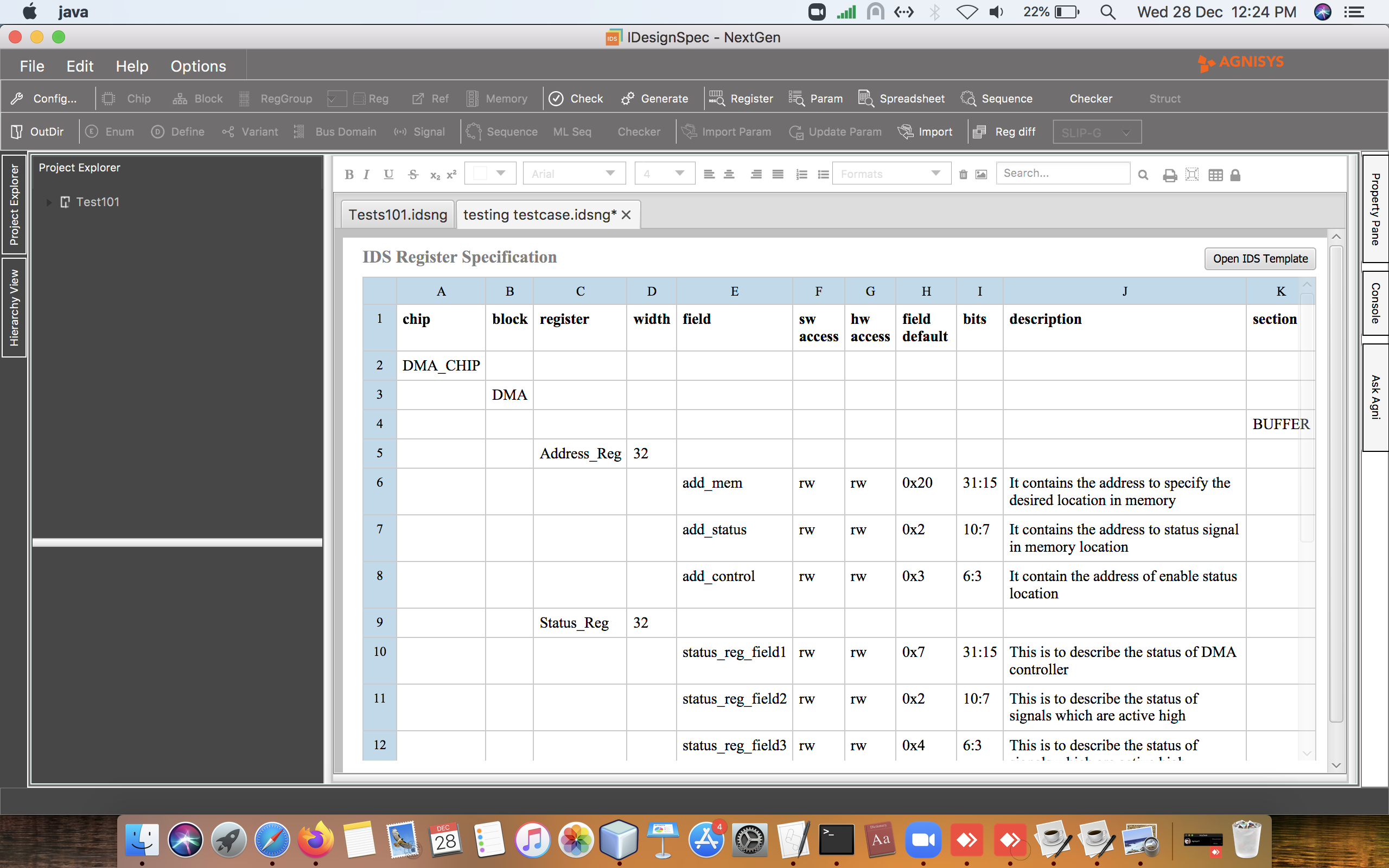
UART Register Map

Conclusion
SLIP-G™ automatically creates register specifications for certain standard IPs with add-in functionality of configurability and customizability, allowing users to configure and customize these IPs to suit their requirements. Agnisys constantly adds new IPs and enhances existing ones to provide ease to the user. Also, all the generated files are available as plain text for easy debugging and use by downstream tools.
Multibit Inference to save Area and Power
Introduction
A multibit component (MBC), such as a 16-bit register, decreases the area and reduces the power in a design. But the essential benefits of MBCs are the creation of a more uniform structure for layout during place and route and the development of the synthesised area of a design.
Multibit inference permits us to outline registers, multiplexers, and three state cells to routinely organised logic or multibit library cells. Multibit library cells (macrocells, such as 16-bit banked flip-flops) have these preferences:
- Littler area and delay, due to shared transistors.
- Decreased clock skew in sequential gates.
- Lower power utilization by the clock in sequential banked components.
- Superior performance, due to the optimised layout inside the MBC.
- Progressed standard layout of the data path.
Example of usage of Synopsys directives:

In the above example there is a top component “store_ram” having two registers “elite_reg” and “impact_reg”. The “elite_reg” register and the field f1 of the “impact_reg” register have the property “synopsys_directive = infer_multibit” applied.
RTL output impact:
//—————————————————————————-
// FIELD : F1
// HW ACCESS : RW WIDTH : 32
// SW ACCESS : RW OFFSET : 0
//—————————————————————–
/*DESCRIPTION : NA
*/
//synopsys infer_multibit elite_reg_f1_q
//—————————————————————————-
// FIELD : F1
// HW ACCESS : RW WIDTH : 16
// SW ACCESS : RW OFFSET : 0
//—————————————————————–
/*DESCRIPTION : {synopsys_directive = infer_multibit}
*/
//synopsys infer_multibit impact_reg_f1_q
always @(posedge clk) begin
The property “synopsys_directive = infer_multibit” is utilized to control multibit inference for all bused registers. Multibit inference of other combinational multibit cells happens only during sequential mapping of multibit registers. Multibit sequential mapping does not drag in as numerous levels of logic as single-bit sequential mapping. In this way, the Design Compiler might not induce a complex multibit sequential cell, such as a JK flip-flop, which might unfavourably affect the quality of the design.
The directive, “synopsys_directive = dont_infer_multibit”, is utilized to disable the mapping of the multibit registers and signals.
Essentially, infer_multibit have the taking after two techniques:
- Direct infer multibit source from HDL source: Usually the finest technique for designers who totally run an introductory synthesis run and after that a quick placement and routing.
- Direct infer multibit from the design mapped: This is the best technique for creators who are familiar with the design’s layout and able to decide where multibit components have the biggest impact.
- Optimization of transistor-level layout.
- It as of now deduced the cause of the routing clog.
Conclusion
IDS now supports the Synopsys directive which is used to enable or disable the “infer_multibit” and “dont_infer_multibit”. This directive is useful for the Synopsys tool VCS compiler for the designers. This is a very useful technique for HDL designers to map the signals in RTL design.
SVGalt2 Output
Introduction
IDS has introduced a new capability using SVG output to represent the specification in a more elegant graphical representation in two dimensional file format. SVG is an extensible Markup Language based vector graphic format for the Web and other environments. The XML code in a SVG file specifies all of the shapes, colours, and text that comprise the image. SVG has several methods that describe lines, curves, shapes, paths, boxes, circles, text, and graphic images.
Usage
IDS provides an easy way to generate SVG Output. To use this feature, svgalt2 keyword is used in output command. The syntax will be as shown below:
idsbatch <filename> -out “svgalt2” -dir <output dir_name/path>
e.g., idsbatch sample1 -out svgalt2 -dir ids
On executing the above command a file with the .htm extension will be generated in the ids folder in its current directory. This file can be opened in any browser.
The key feature of SVG output is the rich look of specification with dynamic GUI which is supported in any browser. SVG output file is stored with the .htm extension.
In the case of chip level only .htm files will be generated with respect to top level component names This has been illustrated in the below image.

This feature supports the chip-in chip feature and for chip level specification an index file is also generated with the name i.e., “index.htm” which contains a table of contents of child components. The details of TOC are linked with its respective SVG output. So, it will be redirected to SVG output on a single click.
Note: This Index.htm should be used for chip in chip case.
Example

Output file will represent chip and block level data with its hierarchical definition in a rectangular box. Each component is mentioned with a box and this box contains component details (i.e., type, name, size, address, offset, end address and bus). Each box is linked with its child component and the child component is able to collapse and expand on a single click on the parent component. This has been illustrated in the below image.

Fig 1: One level of hierarchy (collapsed)

Conclusion
Scalable Vector Graphics (SVG) is a way to render for graphical representation and it helps in understanding the hierarchical connection between each component and has some default data which gives an overview of it. This output is very useful for large data.
Read_Check feature in ISS
Introduction
Oftentimes, in the verification/validation environment, it is required in a test to check whether a value that has been written to a register is the same as the value that has been previously written. If the values are mismatched then an error should be flagged.
A new command in ISS, “read_check” has been supported. In this “read_check” command, the register/field’s hierarchical path will be given in the “step” column, and the value for which the comparison needs to be done will be given in the “value” column. Also, an internal variable will be maintained to keep an error count whose value will increment if any mismatch is encountered for a read check. If any read_check is used in a sequence, at the end of the sequence, a summary of check errors will be displayed.
Sequences:

Firmware Output:
Sequences File:

API File:
read_check is a function that will take the data that is read from the address, the expected data from which the read data needs to be compared with and an errorCount variable. If the data does not match then the errorCount variable is incremented.
Conclusion:
With this feature, it becomes handy to get overall errors about the test sequence. The number of errors encountered in a sequence helps in getting an overall idea of the status of the test which has been run.
IDS FPGA
Introduction
With the continuous advancement of a range of FPGA products in the market, offering the promise of a highly integrated solution with efficiency and reliability is becoming a challenge. Often FPGA designers are faced with challenges like power management, device modeling and increasing I/O performance to match the optimum computational capacity for much complex designs. In addition to this, there is a pressure to deliver these very large designs quickly to save time-to-market.
IDS-FPGA is an integrated solution which is uniquely poised to specifically target FPGA designs to speed up the development while maintaining quality, based on Agnisys’ decade-long experience in specification driven development. This will solve the need of the FPGA designers by providing them an easy-to-use system to design, verify and target the FPGAs.
Salient Features
- Highly configurable solution based on available selected vendors
- A library of predefined IP in HTML format, provided by the selected FPGA vendors is pre-included for easy target and reference
- Integration with Vivado and Quartus
- On the fly special scripts to target selected specific vendors
- Generation verification, firmware, and documentation of target designs
Design usage

Fig 1: New project window to select target vendor

Fig 2: Example design snippet with use of Xilinx UltraScale+ blocks

Fig 3: Tool ‘Project View’ with included created IP, pre-loaded UltraScale+ modules and generated target scripts along with verification, firmware and documentation collaterals
Conclusion
With IDS-FPGA, teams can cut their development time in half using this automated code generation, IP generators, and the smooth integration with the target FPGA vendor software like Xilinx. A high quality and reliable generation of corresponding verification, firmware code as well as documentation for larger designs involving the target FPGAs to ensure consistency of design information among different teams. The future scope would be adding more vendors in the tool to improve the usability factor across a larger group of FPGA design engineers.