Tool for faster AI Chip Development

Transform Your AI Chip Design Process
Discover how our advanced tool IDesignSpec™ can streamline your workflows, enhance productivity, and bring your AI Chips to market faster.
Key Features
Spec Drive Automation
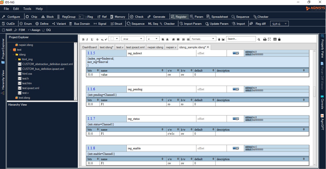
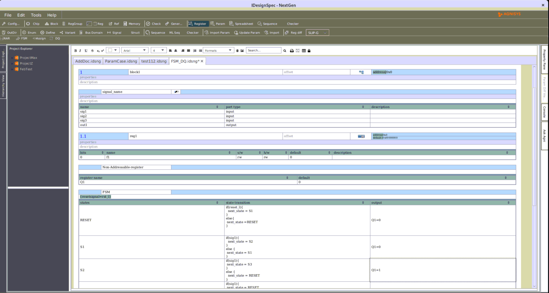
Accelerate chip design with powerful automation of RTL for Designers, UVM for Verification Engineers, C/C++ for Firmware Engineers and Documentation for the entire team.
Fast Register Map Design,
Silicon Proven Bus Interface IP
Your team is more focused on your AI secret sauce so your chips get to your customers faster & at lower cost.
Industry’s Best Support
Timely and efficient responses means your team avoids downtime.
What we do
One of the large sections in any AI chip is the register-map which provides the ability to program the AI engine with weights, parameters, hyper-parameters, etc. These flexible and configurable elements in the AI design are created automatically from a single text based specification. Not just that, the way data moves in and out of these configurable elements is typically done thru standard hardware buses like AMBA, TileLink or CXL. These IPs are created by the Agnisys tool. Some studies suggest a saving of about 30% in time to market.
Advanced areas of chip design such as Clock Domain Crossing, Functional Safety, Low Power, Low Area, High performance are inherently dealt with by Agnisys’ Advanced EDA tool.
Paper : Hardware Based Handwritten Digit Recognition for MNIST
In recent years, hardware acceleration has become a significant area of research for speeding up machine learning tasks, particularly deep learning applications. Field Programmable Gate Arrays (FPGAs) offer unique advantages in terms of parallelism, reconfigurability, and energy efficiency compared to traditional CPU and GPU architectures. The handwritten digit recognition task, particularly using the MNIST dataset, is a classic problem in the machine learning community and serves as a benchmark for evaluating model performance.
This paper focuses on the direct implementation of a handwritten digit recognition model on an FPGA to explore how hardware-based solutions can enhance the speed and efficiency of deep learning models. The primary goal is to detail the FPGA configuration process, data precision handling, and overall performance analysis.
Our Latest Press Release
Etched has made a bold bet that AI transformers would take over the world, and has spent the past two years developing Sohu, the world’s first specialized chip for transformers—the “T” in ChatGPT. Unlike other hardware, Sohu is purpose-built to optimize transformer-based models, outperforming traditional chips that handle a broader range of AI architectures. Etched is burning the transformer architecture directly into the chip, creating the world’s most powerful servers for transformer inference.
What Our Customers Say


Continue Reading
AI/ML in verification
In this webinar, we explored an innovative framework for automated hardware verification using Genetic Algorithms and Value Change Dump (VCD) files. By leveraging evolutionary techniques, we demonstrated how optimized test vectors can efficiently identify anomalies, simplify signal analysis, and enhance verification throughput. designs.
Request Webinar

Request a Live Solution Demonstration
Discover how our advanced tool IDesignSpec™ can streamline your workflows, enhance productivity, and bring your AI Chips to market faster.


